內容表格
沒有標頭原文連結:
http://www.design-reuse.com/articles/15952/raid6-accelerator-in-a-powerpc-iop-soc.html
翻譯 :OSSLab vxr, thx 校對:
摘要/Abstract-- IO Processors (IOP) are key elements for storage application to attach to a Host the maximum number of IO's such as RAID disks, capable for high speed data movement between the Host and these IO's and able to perform function such as parity computation for RAID (Redundant Array of Independent/Inexpensive Disks) applications. A second generation [1] 800MHz PowerPC SOC working with 800MHz DDR2 SDRAM memory and on-chip L2 cache, executes up to 1600 DMIPS is described in this paper. It is designed around an high speed central bus (12.8 GBytes/sec PLB) with crossbar switch capability, integrating 3 PCI express ports, plus one PCI-X DDR interface and RAID 5 & 6 hardware accelerator. The RAID 6 algorithm implement 2 disk parities, with the second Q parity generation based on the finite Galois Field (GF) Primitive Polynomial functions. The SOC has been implemented in a 0.13 um, 1.5 V nominal-supply, bulk CMOS process. Active power consumption is 8W typical when all the IP run simultaneously.
IO Processors (IOP)對於連接主機(Host)上大量IO裝置如RAID磁盤的儲存應用來說是個關鍵要點, 能提供Host與這些IO裝置之間進行高速資料移動並且能執行一些RAID應用的功能, 像是奇偶校驗計算. 這份文件描述了一顆第二代 800MHz SoC, 使用800MHz DDR2 SDRAM記憶體和二階內置快取, 執行運算達到1600DMIPS(Dhrystone MIPS: 一種整數計算運算量的表示方式, 相對於MFLOPS的浮點運算量來說). 這顆SoC被設計圍繞在一條交錯式交換功能(crossbar switch capability)的中央高速匯流排(PLB獲得的頻寬達到12.8GB/s), 整合三組PCI express端口, 增加的一條PCI-X DDR介面和RAID 5&6硬體加速器之中. RAID 6演算法實作2磁盤基偶校驗, 使用基於有限Galois Field (GF)本質多項式產生第二個Q基偶校驗數據( second Q parity). 這顆SoC實作在0.13微米, 標示1.5V電壓, CMOS體積的製程. 當全部的IP(IP core: Intellectual Property core=>指那些特殊的ASIC或著FPGA邏輯電路區塊, 其實就是那些ASIC廠商的硬線產品的相關智產專利部分)運行時,主動式電源消耗典型為8w.
II-介紹/INTRODUCTION
This paper describes a PowerPC system-on-a-chip (SOC) which is intended to address the high-performance RAID market segment. The SOC uses IBM's Core-Connect technology [2] to integrate a rich set of features including a DDRII-800 SDRAM controller, three 2.5Gb/s PCI-Express interfaces[3], hardware accelerated XOR for RAID 5 and RAID 6, I2O messaging, three DMA controllers, a 1Gb Ethernet port, a parallel peripheral Bus, three UARTs, general purpose IO, general purpose timers, and two IIC buses.
這這份文件描述定位於高性能RAID市場領域的Power SoC. SoC使用IBM的Core-Connect技術整合了許多特徵, 包括一組DDRII-800 SDRAM記憶體控制器, 三組2.5Gb/s PCI-Express介面, RAID5/6硬線加速XOR設計, I2O資訊交換(Intelligent I/O), 三組DMA控制器, 一組GbE乙太網路端口, 一組並行周邊匯流排(parallel peripheral Bus), 三組UART, GPI/O介面, 通用計時器(GPT)和兩組IIC匯流排.
II- 系統概觀/SYSTEM OVERVIEW
This SOC design consists of a high performance 32-bit RISC processor core, which is fully compliant with the PowerPC specification. The PowerPC architecture is well known for its low power dissipation coupled with high performance, and it is a natural choice for embedded applications The processor core for this design is based upon an existing, fixed voltage PowerPC 440 core [2]. The core includes a hardware multiply accumulate unit, static branch prediction support, and a 64-entry, fully-associative translation look aside buffer. The CPU pipeline is seven processor stages deep. Single cycle access, 64-way set associative, 32-KByte instruction and data caches are connected to the processor core.
這這顆SoC設計組成一顆完整相容PowerPC規範的高性能32位元RISC處理器核心. PowerPC架構是以低功耗加上高性能, 對於嵌入式應用來說是最佳選擇. 該處理器核心設計是基於現有, 定額電壓的PowerPC 440核心結構. PowerPC 440核心包括了一組MAC(乘法/累加)單元, 支持靜態分支預測和64-entry全關聯式TLB(和Cache相關的設計, 快取命中率的重要部分) . CPU管線深度達到7個階層. 連接在處理器核心的單周期存取(single cycle access), 64路關聯式(64-way set associative), 32KBytes指令快取和資料快取(與PLB連接為128bits; 資料快取是全雙工傳輸架構). 以下方塊圖顯示了兩組IP(Intellectual Property)區塊, 用作為RAID 5和 RAID 6硬體協助高速資料量DMA單元控制.

Figure 1 RAID 5和RAID6的IOP處理器方塊圖 / RAID 5 & 6 IOP processor block diagram
A second level (L2) cache of 256 KB is integrated to improve processor performance. Applications that do not require L2 may optionally use the L2 as on chip SRAM. The L2 memory arrays include redundant bits for parity and spares that can be connected after test and configured with on chip fuses.
第二階256KB快取記憶體被整合用來改進處理器性能. 有些不太需要L2快取的應用, 可以選擇性使用L2快取作為晶片上的SRAM. 經使用晶片保險絲(clip fises)的測試和配置過後, 被連接的L2快取記憶體陣列包括奇偶校驗值和備用值(parity and spares)的冗餘位元部分(redundant bits).
III - 晶片上的高速交錯式匯流排/ON CHIP HIGH SPEED CROSSBAR BUS:
The key element of this SOC for high speed data transfer is the central 128b wide 200 MHz crossbar PLB (Processor Local Bus) [1]. Two out of eleven masters can simultaneously access one of the two PLB slave buses: one specialized in High Bandwidth(HB) data transfer and a second one with Low Latency (LL). The same physical memory in the SDRAM can be accessed either on the HB or the LL slave bus through two aliased address ranges. By convention (but not required) the LL bus segment is used by the PowerPC to achieve low latency access to memory while the HB bus segment is used for large data moves by the DMA engines.
這顆SoC高速資料傳輸的關鍵是128位元寬度, 200MHz的中央交錯式PLB(Processor Local Bus). 11條master中有2條可以同時存取兩條PLB slave匯流排中的一條: 第一條專門負責高頻寬資料傳輸(HB:High Bandwidth data transfer)和第二條用於低延遲(LL: Low Latency)作用. 通過兩個別名位址範圍,不論是在HB或著LL slave匯流排上可以存取在SDRAM中相同的實體記憶體. 按照慣例(非必須), LL匯流排區段透過Power PC被用於實現低延遲記憶體存取, 而HB匯流排區段透過DMA引擎(DMA engine)用於大型資料搬移.
通過兩個別名定址區域, 不論HB或著LL slave匯流排都可以存取在SDRAM上相同的實體記憶體空間. 按照原則(非必須), LL匯流排區段透過使用PowerPC去實現低延遲記憶體存取, 而HB匯流排區段則是透過DMA引擎用於大型資料傳輸.
The Crossbar architecture separates the 64b address, 128b read data, and the 128b write data busses allowing simultaneously duplex operations per master with two independent masters resulting in a peak theoretical bandwidth of 10 Gbytes/sec.
交錯型架構(Crossbar architecture)分成 64位元定址, 128位元讀取資料和128位元寫入資料匯流排, 它使兩條獨立的master能同時雙工操作,最高達到每秒10GB峰值頻寬.
While the Crossbar arbiter supports 64 bit addressing, the PowerPC440 CPU is a 32 bit processor that can address up to 4 GB of physical address, the 64 entry TLB transforms this address to a real 36 bit PLB address (upper 28 bits are 0s) for 64GB access of the total address space.
雖然交錯型仲裁器(Crossbar arbiter)支持64位元定址, 但是PowerPC440 CPU是一顆可以定址到4GB實體位址的的32位元處理器. 64-entry TLB緩衝轉換這個位址到提供總定址空間64GB一個真正的36位元PLB位址, . Raid 5 跟Raid 6 演算法
The RAID 5 have been developed to provide data recovery in the case of a single drive failure by adding a parity disk that is used with the remaining disks to rebuilt the failing data.
RAID 5被開發出用在單一硬碟毀損(failure)情況下提供資料復原功能, 透過使用多餘的磁碟增加一個奇偶校驗磁碟來提供毀損資料(failing data)的重建.
Notice that the Error on a disk drive must be detected by an another error detection circuit such as CRC checking.
注意在一個硬碟上的錯誤(Error)必須透過其他偵錯電路(error detection circuit)像是CRC檢查機制來檢測.
使用Raid 6安全性與可靠性提高
AMCC PowerPC 440SP/440SPe: 皆可支持Raid 5 與Raid 6演算法
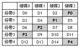
Raid 5運算主要是要計算校驗塊 P ,P求得方式如下
P = D0 Xor D1 Xor D2
下以四顆HDD ,Raid 5會有穿插一顆為P碟(校驗硬碟)
In RAID 6, 雙校驗 P,Q with GF coefficients is needed:
P = D0 Xor D1 Xor D2
Q = (A0×a)⊕(A1×b) ⊕(A2×c)
The RAID 6 algorithm for Q parity generation is based on the Galois Field (GF) Primitive Polynomial functions. With the PPC440SPe it is possible to use several different values of the GF polynomial, including the values 0x11D and 0x14D which corresponds to the equations:
產生Q奇偶校驗值的RAID6演算法是基於Galois Field (GF)原始多項式函數(Primitive Polynomial functions). 使用PPC440SPe可能會使用幾種GF多項式的差異值, 包括對應到方程式(equation)的值-0x11D和值-0x14D:
0x11D: X8 + X4 + X3 + X2 + 1
0x14D: X8 + X6 + X3 + X2 + 1
V - RAID硬體輔助方案/RAID Hardware assist options
There are two options for the RAID hardware assist.
有兩種RAID hardware assist方案.
The fist one is to attach directly to the PLB on chip bus the RAID assist as an independent unit with its own DMA controller and perform the dual P,Q parity between the different operands through the control of the DMA engine.
第一個方案是將自有的DMA控制器直接附著在晶片匯流排PLB上的RAID assist成為獨立的單元, 並且經過DMA引擎控制, 在不同的運算元之間執行雙P,Q奇偶校驗.
The second option is to have this RAID hardware assist directly in the memory controller and enable it if the address on the PLB on chip system bus falls in one predefined address range. In this case some predefined function and parameters must be included in the reserved bits of the 64- bits PLB address.
第二個方案是在記憶體控制器上直接存有這個RAID硬體輔助設計(RAID hardware assist)並且啟用他, 如果晶片匯流排-PLB上該位址落在一個預先定義的定址範圍的話. 在這個情況下, 一些預先定義的函數和參數必須被包含在64位元PLB位址裡的一些保留位元.
VI - PLB上的RAID 5硬體輔助(Hardware assist)/RAID 5 Hardware assist on PLB
The block diagram figure 2 shows that a XOR and Not XOR function is attached directly to the PLB and computes the parity in each cycle when a new operand is entered in the unit.
圖2方塊圖顯示當一個新的運算元被輸入到這個單元時, PLB直接連接一個XOR/NOT XOR功能並且在每個周期計算奇偶校驗值.
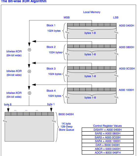
The Hardware XOR engine computes a bit-wise XOR on up to 16 data streams with the results stored in a designated target. The XOR engine is driven by a linked list Command Block structure specifying control information, source operands, target operand, status information, and next link. Source and target can reside anywhere in PLB and/or PCI address space.
硬體XOR引擎使用儲存在指定目標的結果, 在達到16個資料串流(16個單XOR數據)上操作位元運算子-XOR運算(1 xor 2 xor 3 xor 4 xor .... xor n | n=16). XOR引擎透過Command Block架構指定的控制訊息, 來源運算元, 目標運算元, 狀態資訊和下一個鏈結去驅動. 來源和目標可以駐留在PLB和(或著)PCI定址空間裡的任何位址.

Fig 2: DMA aware XOR unit operations
VII - 在記憶體佇列(Memory Queue)中的RAID硬體輔助/RAID Hardware assist in Memory Queue
The block diagram figure 3 show that a XOR and Galois field computation for Q parity is integrated in the Memory Queue of the SDRAM Memory controller. Two circuits are implemented; one working on Writing to the Memory acting like a Read Modify Write, and a second one with a Multiple Read of Data as shown on figure 4.
圖3方塊圖顯示整合在SDRAM記憶體控制器的記憶體佇列(Memory Queue)中一個Q奇偶校驗值的XOR和Galios區域計算. 兩組邏輯電路被實作; 一個是運行在像是一個讀-改-寫(Read Modify Write)操作的記憶體寫入上, 和第二個是使用一種多重資料讀取(Multiple Read of Data)的方式, 如圖4所示.
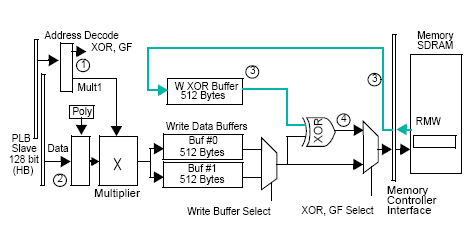
Fig 3: 為RAID 6在記憶體佇列(Memory Queue)中寫入XOR函數/Write XOR function in Memory Queue for RAID 6
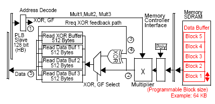
Fig 4: 為RAID 6在記憶體佇列(Memory Queue)中讀取XOR函數/Read XOR function in Memory Queue for RAID 6
The following figures 5 and 6 explain how the address on the PLB is decoded to activate the RAID 5/6 hardware assist in the Memory queue if this address falls in a predefined window.
下面圖5和圖6解釋PLB上的位址如何被解碼後去啟用在記憶體佇列(Memory queue)中的RAID 5/6 硬體輔助(RAID 5/6 hardware assist), 如果這個位址落在預先定義的窗格(window)內的話.

Fig 5: PLB位址去存取在記憶體佇列(Memory Queue)中的RAID 6機制/PLB Address to access RAID 6 function in Memory Queue

Fig 6: 記憶體系統位址/Memory System Address
V - 磁盤條帶操作/Disk STRIP operation
One of the important operation in RAID 5 or 6 is the update of a strip of 64 KB, for example, as illustrated by the following figure 7. The Host that wants to update a strip in the RAID disks has to provide the new data to the IOP in a temporary memory space. Then it is needed to recompute the P and the Q parity. The first step consist in computing a new parity P,Q with the XOR of the current parity and the Strip that will be replaced. Then the P and Q are computed a second time with the new data and the last parity. After all these operations, the new P and Q as the new Data can be send to the Disk controller.
在RAID 5或6中, 重要操作之一是64KB大小的條帶更新, 例如根據下面圖7描述. Host想要更新RAID磁盤裡的條帶必須在暫存記憶體空間裡提供新的資料給IOP. 然後他被用來重新計算P和Q的奇偶校驗(P and the Q parity). 第一步驟在於使用目前的奇偶校驗XOR計算一個新的P, Q奇偶校驗值並且會取代掉條帶數據. 再來P和Q校驗值使用新的資料和最後的奇偶校驗值被計算第二次. 在全部這些操作之後, 新的P和Q校驗值做為新的資料被傳送到磁碟控制器.
These operations are illustrated on the following figure.
這些操作被描述在以下圖中.
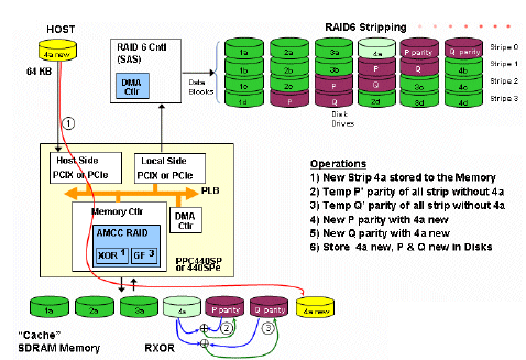
Figure 7: 使用RAID的條帶更新/Strip update with RAID 6
XII- 測試結果/TEST RESULTS
The performance throughput depends on the number of disk drives. The following curve shows one example of throughput for full stripe RAID 6 that has been measured with the PPC440SPe integrating RAID 6 hardware assist.
效能吞吐量取決於磁碟機的數量. 以下曲線圖顯示出一個已使用整合RAID6硬體輔助PPC440SPe測得完整條帶RAID 6吞吐量範例.

Figure 8: 完整條帶RAID 6吞吐量/Full Stripe RAID 6 throughput

Figure 9: 針對RAID性能測試的電路特製板/Board for RAID performance benchmarking
A special board with modular approach for PCI-Express, PCI-X, SDRAM DDR2 DIMMS, and peripheral attachments has been developed. It permits the debug of the SOC device with DDR1 and DDR2 SDRAM as well as PCI Express and PCI-X DDR connectors. Debug was done with the IBM Riscwatch debugger through the JTAG serial link I/O.
一張使用PCI-Express, PCI-X, SDRAM DDR2 DIMMS和周邊附件模組化方式的特製電路板被開發出來. 他允許使用DDR1和DDR2 SDRAM以及PCI Express和PCI-X DDR連接器的SoC裝置除錯.
透過JTAG序列連接I/O, 使用IBM的Riscwatch除錯器工具完成除錯.
XI- SOC IMPLEMENTATION

Figure 10: PowerPC IOP晶片走線/PowerPC IOP Chip layout
主要特徵/Main Features
800MHz PowerPC CPU
256 KB L2 Cache
DDR800 SDRAM Memory Controller
200MHz Internal PLB bus - 12.8GB/s
3 PCI Express Ports (8-4-4 lanes) 2.5Gb/sec per lane
1 PCI-X DDR 266 interface
DMA, I2O, RAID 5 & 6 Hdwr assist, etc.
技術/Technology
CMOS 0.13 um Copper 製程
7 levels of Metal
11.757 million gates
Gate area = 3x12 channels of 0.4um
封裝/Packaging
27mm FC-PBGA (Flip chip Plastic Ball Grid Array)
1mm pitch
495 Signal I/Os
675 Pads
Due to the large number of I/O (495) needed to integrate all the peripherals, the I/Os are placed in an area array across the die. A peripheral approach for IO implementation was possible with a staggered structure; however, it would have resulted in a larger die size, and a more noise sensitive part because of large simultaneous switching.
由於大量的I/O訊號(495條)需要整合全部周邊, I/O訊號配置在一個跨矩陣式晶蕊(die; 晶圓(wafer)切出來的一部分). 對於實作IO週邊的一個方式是使用一種堆疊式架構(Staggered Structure; 一種電晶體結構); 然而, 它將會導致更大的晶蕊面積,和更多的雜訊敏感部分, 因為大量的同時性邏輯轉換關係(Simultaneous Switching: 許多邏輯閘在同時序上瞬間轉態, 會引起更強的SSN).
The device is based on an ASIC with integrated synthesizable cores - also named IP's - with the exception of the PowerPC CPU core which is a precharacterized hard core with optimized timing analysis and tuned clock distribution to achieve 800MHz.
Logic is described in Verilog and synthesis done with Synopsys synthesis tool. The physical design including floorplaning, placement and wiring was done with IBM's proprietary Chip Bench tool. Special care was taken in physical implementation for minimization of noise induced by coupling and simultaneous switching on top of the conventional signal integrity verification.
Extensive simulation of each core with simulation after SOC integration has resulted in a first pass good product.

Figure 11: PowerPC IOP方塊圖/PowerPC IOP block diagram
結論/CONCLUSION
An high performance SOC based on a PowerPC CPU core for RAID storage application, have been tested at 800MHz. with main interfaces such as DDRII SDRAM at 800MHz and three PCI-Express ports. Two RAID hardware accelerators, permits to achieve data throughput in the range of 1 GBytes per second.
針對儲存應用, 一顆基於PowerPC CPU核心的高性能SoC, 使用主要介面像是DDRII 800MHz和三組PCI-Express端口已檢測運行在800MHz. 兩組RAID硬體加速器, 允許實現在每秒1GBytes範圍內的資料吞吐量.
[1] A PowerPC SOC IO Processor for RAID applications, G.Boudon & al. IPSOC04
[2] IBM Corp. (1999) Coreconnect Bus Architecture
[3] "Integrating PCI Express IP in a SoC" Ilya Granovsky, Elchanan Perlin, IP/SOC06
- Was this page helpful?
- 標籤 (Edit tags)
- 什麼連接到這裡
文件 13
| 文件 | 大小 | 日期 | 附件上傳者 | |||
|---|---|---|---|---|---|---|
| amcc_data_in_plb_operation_01.gif 無描述 | 7.69 KB | 09:41, 14 Dec 2011 | vxr | 動作 | |
| amcc_dma_operation_01.gif 無描述 | 13.67 KB | 09:41, 14 Dec 2011 | vxr | 動作 | |
| amcc_memory_stack_01.gif 無描述 | 12.53 KB | 09:41, 14 Dec 2011 | vxr | 動作 | |
| amcc_parity_operation_01.gif 無描述 | 10.39 KB | 09:41, 14 Dec 2011 | vxr | 動作 | |
| amcc_parity_operation_02.gif 無描述 | 12.93 KB | 09:41, 14 Dec 2011 | vxr | 動作 | |
| amcc_parity_raid_process_01.gif 無描述 | 41.85 KB | 09:41, 14 Dec 2011 | vxr | 動作 | |
| amcc_parity_raid_throughput.gif 無描述 | 13.06 KB | 09:41, 14 Dec 2011 | vxr | 動作 | |
| amcc_powerpc_layout_block__01.gif 無描述 | 51.62 KB | 09:41, 14 Dec 2011 | vxr | 動作 | |
| amcc_powerpc_layout_block__02.gif 無描述 | 31.1 KB | 09:41, 14 Dec 2011 | vxr | 動作 | |
| amcc_raid5_6_block_01.gif 無描述 | 11.88 KB | 09:41, 14 Dec 2011 | vxr | 動作 | |
| amcc_raid_hw_show_01.gif 無描述 | 114.43 KB | 09:41, 14 Dec 2011 | vxr | 動作 | |
 | intelraid5.png 無描述 | 81.74 KB | 00:28, 9 Nov 2010 | thx | 動作 | |
| parity_store_process_01.gif 無描述 | 4.94 KB | 09:41, 14 Dec 2011 | vxr | 動作 | |
| Images 13 | ||
|---|---|---|
 |  |  |
 |  |  |
 |  |  |
 |  |  |
 | ||